Hi,
TI DSP C6748 is used in our product now. Three devices are connected to DSP via EMIFA: FPGA(CS5), FLASH(CS2), and Dual-Port RAM(CS4). Our hardware design needs the following configuration: when accessing FLASH, bit 0~3 of PINMUX8 is set to GP3[7]; on the other hand, when accessing FPGA, bit 0~3 of PINMUX8 is set to EMA_D[15]. The GP3[7] is set to INPUT. It is found that the rising rate is slow when switching GP3[7] to EMA_D[15] and that will lead to incorrect results in FPGA.
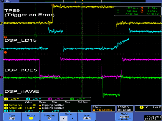
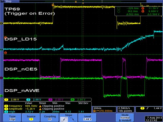
Attached images show the signals in scope for debug: Channel 1 is our internal debug signal, channel 2 is pinmux8 EMA_D[15]/GP3[7], channel 3 is chip select signal, and channel 4 is write enable signal. A slow rising rate of EMA_D[15] ( channel 2, DSP_LD15 ) is observed when DSP_nAWE and DSP_nCE5 signals are triggered. This will lead to incorrect results in FPGA. Can you help to give any advice for us to improve it? Thank you.

